


The President awarded the Prize in “The best invention in product and technology area” for the achievement in blue optoelectronics domain. The Prize was awarded to High Pressure Research Center of PAS prof. Sylwester Porowski and his team
Blue optoelectronics is a new rapidly developing branch of electronics. The predicted blue optoelectronics world market size is 100 billion USD for 2006-2008. The main applications include: dense storage of information, generation of high quality full color pictures, new generation of energy-saving light sources, numerous application in medicine, environment protection, military areas.
This branch relies on the use of new semiconductor, gallium nitride GaN. This material is extremely difficult to synthesize in the form of high quality crystals, necessary for applications. In Poland a new high pressure GaN synthesis method has been invented and patented. This method is capable to provide highest quality material in the world. This assured to Poland an excellent competitive position and prestige in this important area.
These achievements led to the establishment of Strategic State Program “Development of Blue Optoelectronics”. The Program, planned for years 2000-2004, is financed in 30% by the state and in 70% by private funds. It is anticipated in the Program that the blue optoelectronic devices, such as blue lasers and UV detectors will be produced in Poland. It is estimated that Poland has the chance to capture 1-2% share of world market of blue optoelectronics, i.e. 2 billon USD.
The availability of the best GaN crystals allowed to construct blue laser in Poland in record short time of 14 months. In HPRC, the first in the world dislocation free semiconductor laser started to operate on 12 Dec 2001.
|
|
|
|
|
|
|
|
|
|
|
|
|
|
|
|
|
|
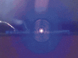
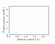
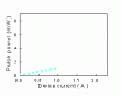
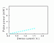
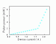
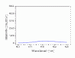
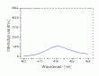
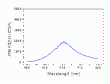
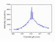
Fig. 1. Optical emission of laser for increasing device current. Upper row – video camera view, middle – total optical output, bottom row – laser emission spectra .
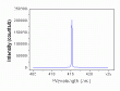
The blue laser constructed in HPRC is a laser diode containing In0.09Ga0.91N/In0.01Ga0.99N 5 repetition Multiple Quantum Well> the diode emits the light in 410-420 nm wavelength range. The optically active layer is stacked between two 0.1 m m GaN:Si and GaN:Mg waveguiding layers. The n-type cladding is 120 repetition 25Å/25Å GaN/Al0.15Ga0.85N silicon doped superlattice. P-type cladding is formed by Mg doped 0.36 m m thick Al0.08Ga0.92N layer. The structure is capped by 0.1 m m highly Mg doped GaN contact layer. The device was processed as narrow stripe, oxide isolated laser. The stripe width is 10 m m.
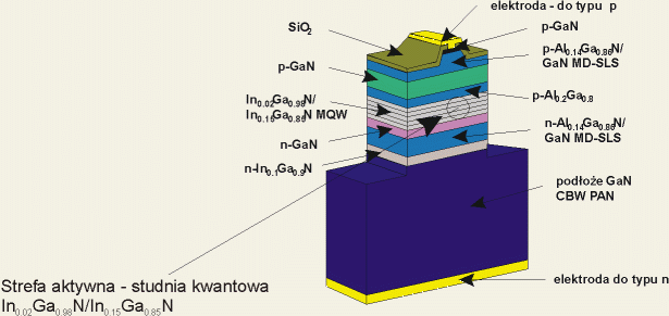
Fig 2. The design of HPRC blue laser
HPRC technology allowed to obtain the devices, having 100,000 smaller density of detrimental crystallographic structure defects – dislocations, than in the best devices obtained using other technologies. Therefore HPRC blue laser contains no dislocation in the active layer. Other best laser diodes have, in average, about 100 dislocations in this layer. Construction of dislocation-free laser diode opens the route to high power lasers and also completely new types of lasers such as cascade and polariton lasers. On the contrary, even the presence of single dislocation makes impossible the action of high power lasers and also the cascade and polariton lasers.
The most important new applications of high power lasers include daylight laser projectors, environment protection and detection of biological and chemical weapons, of the cascade lasers – telecommunication and of the polariton lasers – optical processing of information and optical computing. Entirely new medical applications open for a new device “lab on a chip” – designed for fast analysis of biological materials.
Constructed in HPRC laser opens a number of new possibilities, not accessible to competing lasers constructed on sapphire substrates. In the next ten years, the development of this technology will result in creation of tens of high-tech companies in Poland
High Pressure Research Center of Polish Academy of Sciences has been established in 1972 by spinning off the High Pressure Laboratory of Institute of Physics of PAS. The scientific program has been formulated in collaboration with many distinguished scientists, e.g. prof. Maciej Grabski of Warsaw University of Technology, prof. William Paul of Harvard University and prof. Leonard Sosnowski of Warsaw University. The basic feature of the program was optimal combination of basic and applied research and also the development of new equipment and research methods in high pressure domain. The purpose of the research has been the application of extremely high pressures to determination of the properties and the creation of the materials. In the beginning, the main direction was the investigation of the properties of semiconductors, ceramics and plastically formed metals. In the later years this has been supplemented by addition of the investigation of nanomaterials and biological materials under pressure. At present in HPRC 86 people is employed, including about 50 scientific workers.
The main building of HPRC is located in Warsaw at Sokołowska 29/37. The Center has also New Technologies Building located in Warsaw, Prymasa Tysiaclecia Ave and division in Celestynów.
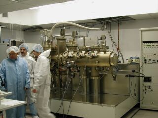
Fig 3. MBE growth apparatus, in HPRC in Warsaw, Prymasa Tysiaclecia Ave. The equipment has been used in the creation of blue laser.

Fig. 4. President of Poland, Mr Aleksander Kwasniewski, awarded the prize for "The best discovery in the field of product or technology" to Prof. Sylwester Porowski and his research team. Poznan, 18 June 2002
HPRC contact address is: 01-142 Warsaw, Sokołowska 29/37, tel 632-50-10, fax: 632-42-18, e-mail: sylvek@unipress.waw.pl, http://www.unipress.waw.pl . The management: director prof. Sylwester Porowski, deputy director prof. Bogdan Pałosz.